Project 2: A RV32C Toy CPU
IMPORTANT INFO - PLEASE READ
The projects are part of your design project worth 2 credit points. As such they run in parallel to the actual course. So be aware that the due date for project and homework might be very close to each other! Start early and do not procrastinate.
Overview
In this individual project, you will embark on a two-step journey to create a toy RVC CPU. Before diving into the task, please pay close attention to the following important points:
Any behavior that violates course rules is strictly prohibited. This includes viewing, copying or plagiarizing other individuals’ circuits and codes. Violators will face severe consequences
You are allowed to use any built-in blocks of Logisim, except for the System On a Chip group, throughout this project.
Save frequently and commit frequently! Try to save your code in Logisim every 5 minutes or so, and commit every time you produce a new feature, even if it is small.
Don’t move around the given inputs and outputs in your circuit; this could lead to issues with the autograder.
Introduction
This excerpt from the RISC-V User-Level ISA Specification describes the current draft proposal for the RISC-V standard compressed instruction set extension, named “C”, which reduces static and dynamic code size by adding short 16-bit instruction encodings for common operations. The C extension can be added to any of the base ISAs (RV32, RV64, RV128), and we use the generic term “RVC” to cover any of these. Typically, 50%–60% of the RISC-V instructions in a program can be replaced with RVC instructions, resulting in a 25%–30% code-size reduction. In this project, we will build a CPU that solely supports some of the RVC instructions.
Project 2.1: Implement CI and CR type instructions (DDL: May 7th)
In this part, your task involves implementing all CI and CR type instructions shown in The Instruction Set below. Feel free to refer to the advice provided in the How to Get Started section to kickstart your circuit adventure.
Project 2.2: Implement all instructions (DDL: May 26th)
In this part, you need to implement all instructions shonw in The Instruction Set table below. Notice: A new template is provided for you to implement the instructions. You can copy and paste your circuit from the previous part to save time.
The Instruction Set
The instructions you need to implement are shown in the table below:
| Format | ISA | OP[1:0] | Funct3 | Implementation |
|---|---|---|---|---|
| CR | add | 10 | 100 | x[rd] = x[rd] + x[rs2] |
| CR | mv | 10 | 100 | x[rd] = x[rs2] |
| CI | addi | 01 | 000 | x[rd] = x[rd] + sext(imm) |
| CI | slli | 10 | 000 | x[rd] = x[rd] << uimm |
| CI | li | 01 | 010 | x[rd] = sext(imm) |
| CI | lui | 01 | 011 | x[rd] = sext(imm[17:12] << 12) |
| CI | nop | 01 | 000 | None |
| CSS | swsp | 10 | 110 | M[x[2] + uimm][31:0] = x[rs2] |
| CIW | addi4spn | 00 | 000 | x[8+rd’] = x[2] + nzuimm |
| CL | lw | 00 | 010 | x[8+rd’] = sext(M[x[8+rs1’] + uimm][31:0]) |
| CS | sw | 00 | 110 | M[x[8+rs1’] + uimm][31:0] = x[8+rs2’] |
| CB | beqz | 01 | 110 | if (x[8+rs1’] == 0) pc += sext(offset) |
| CJ | j | 01 | 101 | pc += sext(offset) |
| CR | jr | 10 | 100 | pc = x[rs1] |
A detailed description of compressed instruction formats is provided in The RISC-V Compressed Instruction Set Manual, Version 1.9. Some important information is also provided below. Please note that there are different versions of RVC instructions, and referencing other documents or webpages may result in failing the test.
Instruction Formats
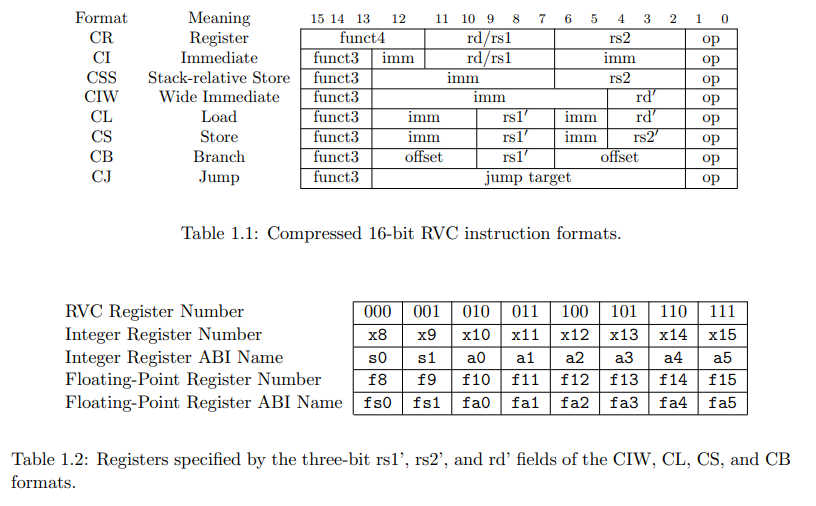
Table 1.1 shows the eight compressed instruction formats. CR, CI, and CSS can use any of the 32 RVI registers, but CIW, CL, CS, and CB are limited to use only 8 of them, which are registers x8 to x15 listed in Table 1.2. In project 2, you do not need to implement all 32 registers, please refer to the Restriction section for details.
Tips: you can try to decode the instruction to opcode, register address, immediate and so on firstly.
CR Format
| CR | FUNCT4 | RD/RS1 | RS2 | OPCODE |
|---|---|---|---|---|
| Bits | 4 | 5 | 5 | 2 |
| C.ADD | 1001 | dest≠ 0 | src≠ 0 | 10 |
| C.MV | 1000 | dest≠ 0 | src≠ 0 | 10 |
| C.JR | 1000 | src≠ 0 | 0 | 10 |
CI Format
| CI | FUNCT3 | IMM | RD/RS1 | IMM | OPCODE |
|---|---|---|---|---|---|
| Bits | 3 | 1 | 5 | 5 | 2 |
| C.LI | 010 | imm[5] | dest≠ 0 | imm[4:0] | 01 |
| C.LUI | 011 | nzimm[17] | dest≠{0,2} | nzimm[16:12] | 01 |
| C.ADDI | 000 | nzimm[5] | dest≠ 0 | nzimm[4:0] | 01 |
| C.SLLI | 000 | shamt[5] | dest≠ 0 | shamt[4:0] | 10 |
CL Format
| CL | FUNCT3 | IMM | RS1’ | IMM | RD’ | OPCODE |
|---|---|---|---|---|---|---|
| Bits | 3 | 3 | 3 | 2 | 3 | 2 |
| C.LW | 010 | offset[5:3] | base | offset[2|6] | dest | 00 |
CS Format
| CS | FUNCT3 | IMM | RS1’ | IMM | RS2’ | OPCODE |
|---|---|---|---|---|---|---|
| Bits | 3 | 3 | 3 | 2 | 3 | 2 |
| C.SW | 110 | offset[5:3] | base | offset[2|6] | src | 00 |
CSS Format
| CSS | FUNCT3 | IMM | RS2’ | OPCODE |
|---|---|---|---|---|
| Bits | 3 | 6 | 5 | 2 |
| C.SWSP | 110 | offset[5:2|7:6] | src | 10 |
CIW Format
| CIW | FUNCT3 | IMM | rd’ | OPCODE |
|---|---|---|---|---|
| Bits | 3 | 8 | 3 | 2 |
| C.ADDI4SPN | 000 | zimm[5:4|9:6|2|3] | dest | 00 |
CJ Format
| CJ | FUNCT3 | JUMP TARGET | OPCODE |
|---|---|---|---|
| Bits | 3 | 11 | 2 |
| C.J | 101 | offset[11|4|9:8|10|6|7|3:1|5] | 01 |
CB Format
| CB | FUNCT3 | IMM | RD’/RS1’ | IMM | OPCODE |
|---|---|---|---|---|---|
| Bits | 3 | 3 | 3 | 5 | 2 |
| C.BEQZ | 110 | offset[8|4:3] | src | offset[7:6|2:1|5] | 01 |
TOP I/O
The inputs and outputs of top level are fixed in TOP circuit. It’s not allowed to add extra pins in TOP circuit in your submission. Fail to comply with this may result in losing all your points!
| Type | signal | bit width | description |
|---|---|---|---|
| input | clk | 1 | clock |
| input | rst | 1 | reset |
| input | inst | 16 | RVC instruction |
| input | mem_dout | 32 | data from memory |
| input | current_pc | 32 | current pc value |
| output | mem_wen | 1 | memory write enable |
| output | mem_din | 32 | data written to memory |
| output | mem_ren | 1 | memory read enable |
| output | mem_addr | 32 | address of memory |
| output | control_en | 1 | enable writing value to pc |
| output | control_pc | 32 | value written to pc |
| output | wb_en | 1 | regfile write enable |
| output | wb_addr | 5 | address written to regfile |
| output | wb_data | 32 | data written to regfile |
Some of these pins are not involved in Project 2.1 but will be used in Project 2.2, so you can temporarily ignore them.
Fetch
Throughout this project, you will work with the Fetch module provided by the TA. This module assumes that
- The instruction memory is halfword-addressable, i.e., each address refers to a 16-bit memory space.
- During each clock cycle, an instruction is fetched from the address stored in the program counter.
- The address value in the program counter increments by one each clock cycle to fetch the next instruction without considering branch or jump.
Additionally, you have the flexibility to incorporate sub-circuits to explore the functionality of the Fetch module. Doing so will enhance your understanding of its operational principles.
How to get start
Here is a simple template to get started. Please download and unzip it first. Opening proj_2_1.circ with logisim-evolution, you will find several subcircuits inside it.
For project 2.2, you can use this template to get started.
- TOP is the top-level circuit you need to complete. It represents the implementation of the target toy CPU that includes the subcircuits you designed. Please note that do not modify the packaging of the TOP circuit or any parts marked as “Don’t touch”, as failing to comply with this may result in failing the test cases.
- testbench is a completed circuit provided by TAs for testing purposes. You can write any binary format instruction to the ROM and observe whether your circuit operates as expected. This circuit will not be used in grading, so feel free to make any attempts.
Here are some suggestions for your information:
- It’s recommended that try to implement instructions one by one and you can start with LI or LUI instructions! This method is debug-friendly.
- List all the signals you need, and try to classify them into different groups. Classifying signals helps complete circuits in the simplest way. You will find that the workload is much smaller in this way.
Test
Test for all CR and CI type instruction has been included with the template package. You can run it with the command./test.sh. The provided test case is carried out in the order (LI-LI-LUI-LUI-SLLI-ADD-MV-ADDI-ADDI), and errors in the previous instructions may result in incorrect results in the later ones even if you implement them correctly.
The 8000 instruction utilizes a reserved instruction space to generate the halt signal. This signal serves the same purpose as the halt signal in Lab 5, which is to terminate the execution of the auto-test script. While this signal is crucial for the auto-test script, it does not produce any additional effects. Please be aware that when the 8000 instruction is executed, your system should not generate any significant output. The Autograder will not evaluate the output of this instruction.
In submission, you need to correctly implement at least one of LI or LUI to ensure that the other instructions can be successfully tested.
Notice: The Autograder of project 2.2 will test all instruction shown in the Instruction Set.
Restriction
In order to reduce your workload and help you pass the test smoothly, some restrictions are stipulated as follows. You should read this section carefully as it may not be consistent with the content in the Instruction Set Manual.
All data is represented in 2’s complement form.
The data memory (RAM) is word-addressable, i.e., each address refers to a 32-bit memory space.
The Autograder will reset your system before carrying out any instructions. In other words, during the first cycle, all pins should output 0.
To reduce your workload, all test scripts will only involve ten integer registers x0, x2, x8-x15.
All instructions in testcases are valid, and you don’t need to consider instruction checking (please note that NOP is also a valid instruction in RVC and our CPU).
Since logisim supports memory with limited size, only the lower 8 bits of an 32-bit address are used to access instruction memory (ROM) and lower 16 bits to access data memory (RAM).
In project 2.1 are,
Siting Liu <liust AT shanghaitech.edu.cn>
Yutong Wang <wangyt32023 AT shanghaitech.edu.cn>
and
Suting Chen <chenst AT shanghaitech.edu.cn>
In project 2.2 are,
Siting Liu <liust AT shanghaitech.edu.cn>
and
Yutong Wang <wangyt32023 AT shanghaitech.edu.cn>
Last modified: 2024-05-12