Goals
-
Understand the structure of a shift and add multiplier.
-
Implement a non-pipelined 4-bit shift and add multiplier.
-
Implement a pipelined 4-bit shift and add multiplier.
Lab 8
Computer Architecture I ShanghaiTech University
Lab 8
PipeLine
Setup
- Download source code from here
Warmup
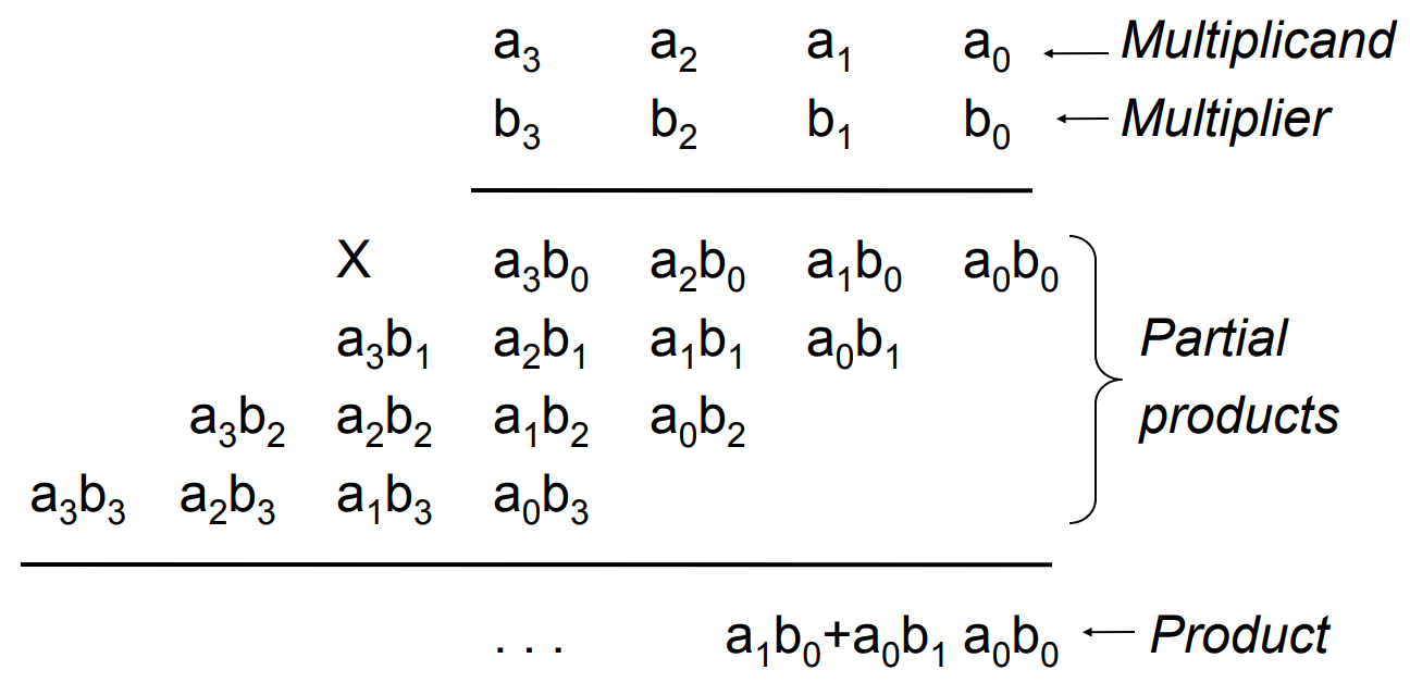
Recall multiplication by hand:

Similarly to calculating by hand, multipliers find a way to sum up all partial products. Many different circuits exist for multiplication. Each one has a different balance between speed (performance) and amount of logic (cost). Today, we are going to implement and optimize one of the most basic multiplier: shift and add multiplier.
Shift and Add Multiplier
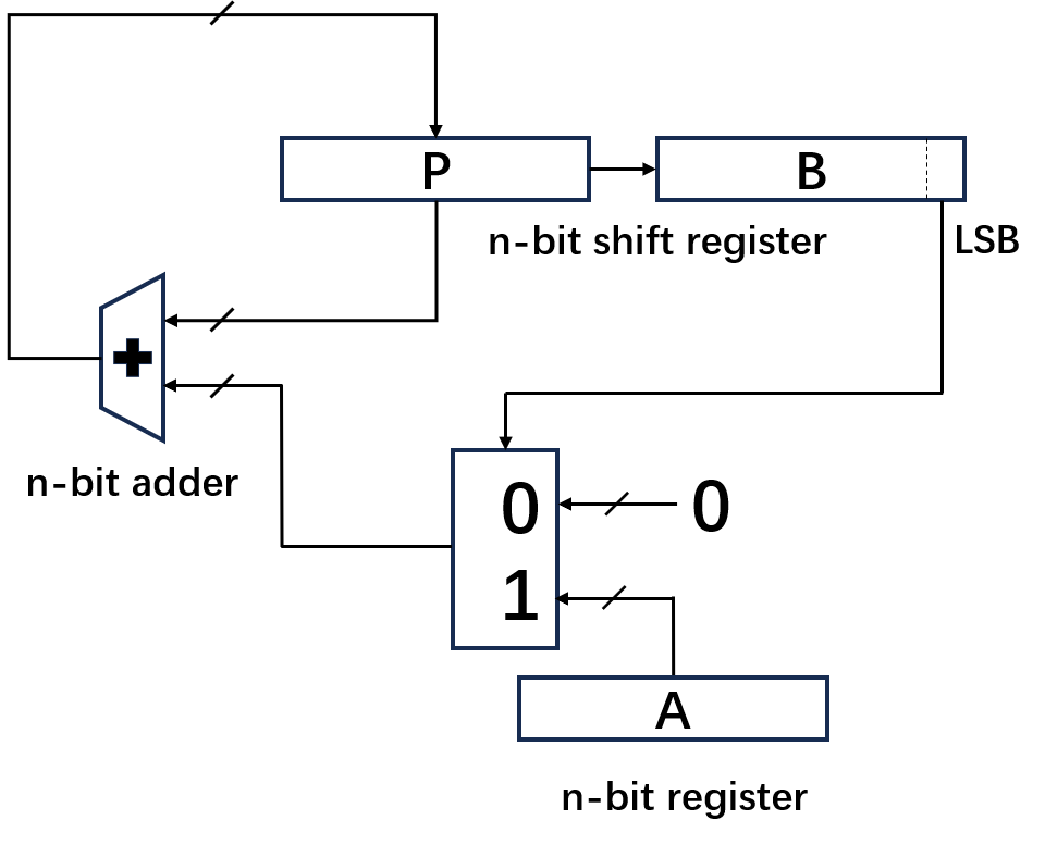
Here we review the structure of shift and add multiplier:

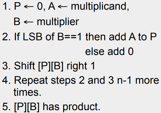
The Controal Algorithm of the shift and add multiplier is:

In this practice, we assume that the multiplier and multiplicand are 4-bit unsigned integers, and the output is an 8-bit unsigned integer. Hence the whole multiplier can be flattened to a combined logic.
1. non_pipelined 4-bit shift and add multiplier
We're going to finish a non-pipelined 4-bit shift and add multiplier in this section.
Action Item
Complete the following steps (remember to save often):
-
Open up the Exercise 1 schematic (
File->Open->Lab8.circ) and go to theshift_and_addcircuit. -
Connect all components to implement a single shift and add step. Once you finished, the circuit should correctly decide whether to add or not to add the input multiplicand on the current result, and output the shifted multiplicand as well.
Hint: We are going to shift the multiplicand here. Take a look at the control algorithm again and think carefully about the shift direction.
-
Now refer to the
non-pipelinedcircuit. Play with the inputs to see if your implementation is correct, and adjust your design if necessary. -
Let the propagation delay of an adder block be 45 ns, the propagation delay of a MUX be 20 ns, and the propagation delay of a shifters block be 5 ns (since we have a constant offset, it is very efficient). The register has a CLK-to-Q delay of 10 ns, a setup time of 10 ns, and a hold time of 5 ns. Calculate the maximum clock rate at which this circuit can operate, assuming that both inputs come from clocked registers that receive their data from an external source.
Checkoff
- Show your design and the highest clock rate achieved to your TA.
2. Pipe that line
The shift-addition multiplier we implemented exhibits significant inefficiencies. Consider dividing the implementation into two stages to maximize its clock rate. Note that to pipeline the circuit, we need registers to hold the intermediate values of the computation between pipeline stages. This requirement is a general theme with pipelines.
To verify that your pipelined design still produces correct outputs, we will consider the outputs from the circuit "correct" if and only if they match the sequence of outputs the non-pipelined version would emit, except for some leading zeros. This leading zero occurs because the second stange of the pipeline is "empty" in the first cycle. For example, if the non-pipelined version produces the sequence [3, 5, 1, 2, 4, …], a correct pipelined circuit might produce the sequence [0, 3, 5, 1, 2, 4, …] for the same series of inputs. You can check this by simulating the circuit and either advancing the clock manually or enabling continuous ticks.
Note: You should run this simulation in the main circuit. You can modify the inputs by right-clicking the ROM and selecting Edit Contents.
Action Item
- Complete the design of
pipelined.circ. You may only add registers to separate stages. - Calculate the maximum clock rate for the pipelined version of the circuit you designed.
Checkoff
- Show your design and the highest clock rate achieved to your TA.
The following TA(s) are responsible for this lab:
Xinxin Yu