Principle of Locality
When a student who is researching something gathers several relevant books on a library desk, he create a localized, easily accessible pool of memory, reducing the need to constantly retrieve additional materials.
Just as the student did not need to access all the books in the library at once with equal probability, a program does not access all of its code or data at once with equal probability.
This mirrors the principle of locality in computer memory, where programs access a relatively small portion of their address space at any instant oftime, just as you accessed a very small portion of the library's collection.
There are two different types of locality:
-
Temporal locality (locality in time): if an item is referenced, it will tend to be referenced again soon. If you recently brought a book to your desk to look at, you will probably need to look at it again soon.
-
Spatial locality (locality in space): if an item is referenced, items whose addresses are close by will tend to be referenced soon.
Just as accesses to books on the desk naturally exhibit locality, locality in programs arises from simple and natural program structures.
For example, most programs contain loops, so instructions and data are likely to be accessed repeatedly, showing large temporal locality.
Since instructions are normally accessed sequentially, programs also show high spatial locality. Accesses to data also exhibit a natural spatial locality. For example, sequential accesses to elements of an array or a record will naturally have high degrees of spatial locality.
Memory Hierarchy
We take advantage of the principle of locality by implementing the memory of a computer as a memory hierarchy. A memory hierarchy consists of multiple levels of memory with different speeds and sizes. The faster memories are more expensive per bit than the slower memories and thus are smaller.
Below is the basic structure of a memory hierarchy:
| Name | Speed | Size | Cost ($/bit) | Technology |
|---|---|---|---|---|
| Cache | Fastest | Smallest | Highest | SRAM |
| Main Memory | Medium | Medium | Medium | DRAM |
| Storage | Slowest | Biggest | Lowest | Magnetic Disk / NAND Flash |
The data are similarly hierarchical: a level closer to the processor is generally a subset of any level further away, and all the data are stored at the lowest level. By analogy, the books on your desk form a subset of the library you are working in, which is in turn a subset of all the libraries on campus. Furthermore, as we move away from the processor, the levels take progressively longer to access, just as we might encounter in a hierarchy of campus libraries.
A memory hierarchy can consist of multiple levels, but data are copied between only two adjacent levels at a time, so we can focus our attention on just two levels.
The minimum unit of information that can be either present or not present in the two-level hierarchy is called a block or a line; in our library analogy, a block of information is one book.
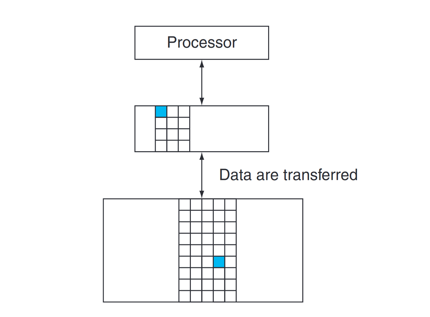
If the data requested by the processor appear in some block in the upper level, this is called a hit (analogous to your finding the information in one of the books on your desk). If the data are not found in the upper level, the request is called a miss. The lower level in the hierarchy is then accessed to retrieve the block containing the requested data. (Continuing our analogy, you go from your desk to the shelves to find the desired book.) The hit rate, or hit ratio, is the fraction of memory accesses found in the upper level; it is often used as a measure of the performance of the memory hierarchy. The miss rate (1−hit rate) is the fraction of memory accesses not found in the upper level.
Since performance is the major reason for having a memory hierarchy, the time to service hits and misses is important. Hit time is the time to access the upper level of the memory hierarchy, which includes the time needed to determine whether the access is a hit or a miss (that is, the time needed to look through the books on the desk). The miss penalty is the time to replace a block in the upper level with the corresponding block from the lower level, plus the time to deliver this block to the processor (or the time to get another book from the shelves and place it on the desk).
The Big Picture
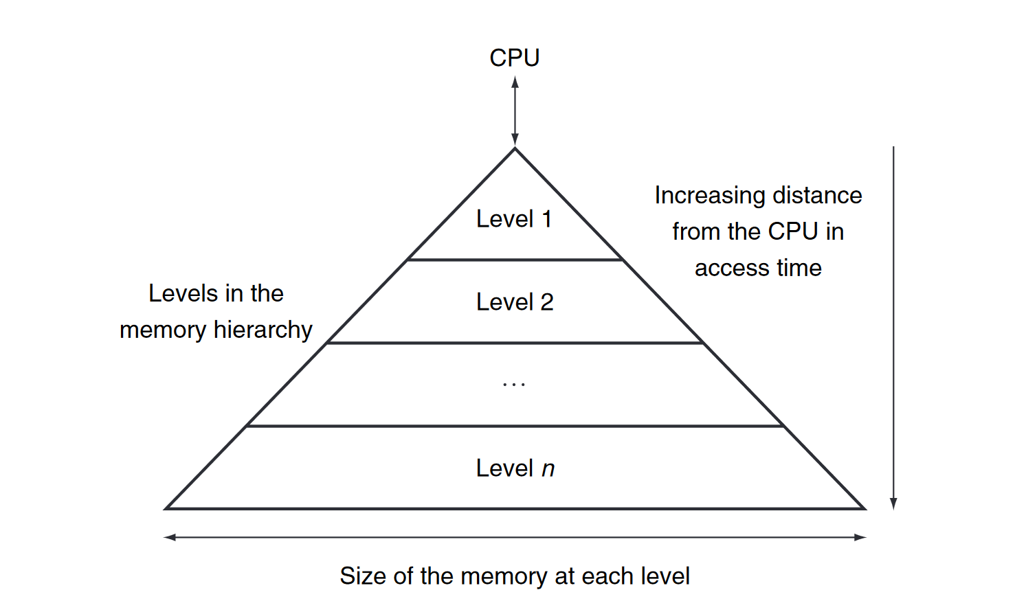
Below shows that a memory hierarchy uses smaller and faster memory technologies close to the processor. Thus, accesses that hit in the highest level of the hierarchy can be processed quickly. Accesses that miss go to lower levels of the hierarchy, which are larger but slower. If the hit rate is high enough, the memory hierarchy has an effective access time close to that of the highest (and fastest) level and a size equal to that of the lowest (and largest) level.
Memory Technologies
There are four primary technologies used today in memory hierarchies. Main memory is implemented from DRAM, while levels closer to the processor (caches) use SRAM. The third technology is flash memory. This nonvolatile memory is the secondary memory in Personal Mobile Devices. The fourth technology, used to implement the largest and slowest level in the hierarchy in servers, is magnetic disk. However, nowadays in 2024, the SSD (flash) is rapidly replacing the position of the HDD (magnetic disk).
Previously in "The Basics of Logic Design", we've introduced the low-level implementation of SRAM and DRAM, this time we'll more focus on the high-level details along with the flash and magnetic disk.
| Memory technology | Typical access time | $ per GiB in 2012 |
|---|---|---|
| SRAM semiconductor memory | 0.5-2.5 ns | $500-$1000 |
| DRAM semiconductor memory | 50-70 ns | $10-$20 |
| Flash semiconductor memory | 5,000-50,000 ns | $0.75-$1.00 |
| Magnetic disk | 5,000,000-20,000,000 ns | $0.05-$0.10 |
SRAM Technology
SRAMs are simply integrated circuits that are memory arrays with (usually) a single access port that can provide either a read or a write. SRAMs have a fixed access time to any datum, though the read and write access times may differ.
SRAMs don't need to refresh and so the access time is very close to the cycle time. SRAMs typically use six to eight transistors per bit to prevent the information from being disturbed when read. SRAM needs only minimal power to retain the charge in standby mode.
In the past, most PCs and server systems used separate SRAM chips for either their primary, secondary, or even tertiary caches. Today, thanks to Moore's Law, all levels of caches are integrated onto the processor chip, so the market for independent SRAM chips has nearly evaporated.
DRAM Technology
In a SRAM, as long as power is applied, the value can be kept indefinitely. In a dynamic RAM (DRAM), the value kept in a cell is stored as a charge in a capacitor. A single transistor is then used to access this stored charge, either to read the value or to overwrite the charge stored there. Because DRAMs use only one transistor per bit of storage, they are much denser and cheaper per bit than SRAM. As DRAMs store the charge on a capacitor, it cannot be kept indefinitely and must periodically be refreshed. That is why this memory structure is called dynamic, in contrast to the static storage in an SRAM cell.
To refresh the cell, we merely read its contents and write it back. The charge can be kept for several milliseconds. If in every clock we could only refresh one bit, we would constantly be just refreshing the DRAM, leaving no time for really use it. Fortunately, DRAMs use a two-level decoding structure, and this allows us to refresh an entire row (which shares a word line) with a read cycle followed immediately by a write cycle.
To improve performance, DRAMs buffer rows for repeated access. The buffer acts like an SRAM; by changing the address, random bits can be accessed in the buffer until the next row access. This capability improves the access time significantly, since the access time to bits in the row is much lower.
To improve the interface to processors further, DRAMs added clocks and are properly called synchronous DRAMs or SDRAMs. The advantage of SDRAMs is that the use of a clock eliminates the time for the memory and processor to synchronize. The speed advantage of synchronous DRAMs comes from the ability to transfer the bits in the burst without having to specify the address of data bits. Instead, the clock transfers the successive bits in a burst. Without a global clock to synchronize operations, each access to memory would require its own control signals and potentially its own address specification.
The fastest version is called Double Data Rate (DDR) SDRAM. The name means data transfers on both the rising and falling edge of the clock, thereby getting twice as much bandwidth as you might expect based on the clock rate and the data width.
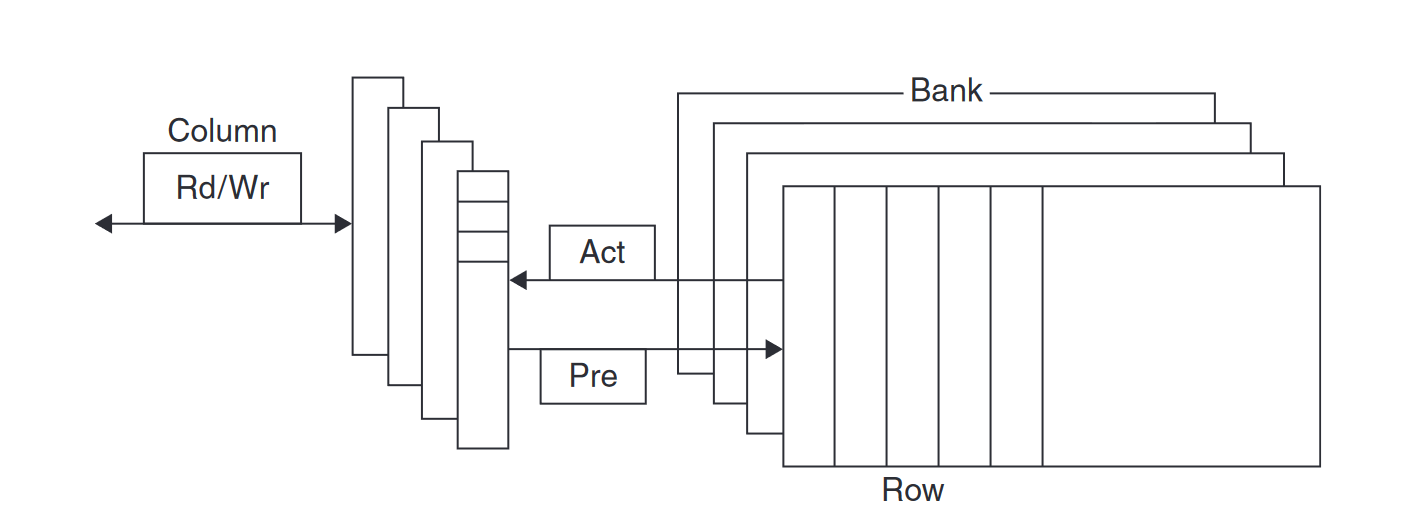
Sustaining that much bandwidth requires clever organization inside the DRAM. Instead of just a faster row buffer, the DRAM can be internally organized to read or write from multiple banks, with each having its own row buffer. Sending an address to several banks permits them all to read or write simultaneously. For example, with four banks, there is just one access time and then accesses rotate between the four banks to supply four times the bandwidth. This rotating access scheme is called address interleaving.
Modern DRAMs are organized in banks, typically four for DDR3. Each bank consists of a series of rows. Sending a Pre (precharge) command opens or closes a bank. A row address is sent with an Act (activate), which causes the row to transfer to a buffer. When the row is in the buffer, it can be transferred by successive column addresses at whatever the width of the DRAM is (typically 4, 8, or 16 bits in DDR3) or by specifying a block transfer and the starting address. Each command, as well as block transfers, is synchronized with a clock.
Flash Memory
Flash memory is a type of electrically erasable programmable read-only memory (EEPROM). Unlike disks and DRAM, but like other EEPROM technologies, writes can wear out flash memory bits. To cope with such limits, most flash products include a controller to spread the writes by remapping blocks that have been written many times to less trodden blocks. This technique is called wear leveling. With wear leveling, personal mobile devices are very unlikely to exceed the write limits in the flash. Such wear leveling lowers the potential performance of flash, but it is needed unless higher-level software monitors block wear. Flash controllers that perform wear leveling can also improve yield by mapping out memory cells that were manufactured incorrectly.
Disk Memory
As below shows, a magnetic hard disk consists of a collection of platters, which rotate on a spindle at 5400 to 15,000 revolutions per minute. The metal platters are covered with magnetic recording material on both sides, similar to the material found on a cassette or videotape. To read and write information on a hard disk, a movable arm containing a small electromagnetic coil called a read-write head is located just above each surface. The entire drive is permanently sealed to control the environment inside the drive, which, in turn, allows the disk heads to be much closer to the drive surface.
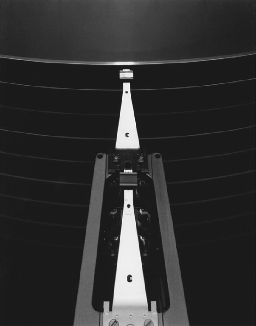
Each disk surface is divided into concentric circles, called tracks. There are typically tens of thousands of tracks per surface. Each track is in turn divided into sectors that contain the information; each track may have thousands of sectors. Sectors are typically 512 to 4096 bytes in size. The sequence recorded on the magnetic media is ... | a sector number | a gap | the information for that sector including error correction code | a gap | the sector number of the next sector | ..., and so on.
The disk heads for each surface are connected together and move in conjunction, so that every head is over the same track of every surface. The term cylinder is used to refer to all the tracks under the heads at a given point on all surfaces.
To access data, the operating system must direct the disk through a three-stage process. The first step is to position the head over the proper track. This operation is called a seek, and the time to move the head to the desired track is called the seek time.
Once the head has reached the correct track, we must wait for the desired sector to rotate under the read/write head. This time is called the rotational latency or rotational delay. The average latency to the desired information is halfway around the disk. Disks rotate at 5400 RPM to 15,000 RPM. The average rotational latency at 5400 RPM is:
The last component of a disk access, transfer time, is the time to transfer a block of bits. The transfer time is a function of the sector size, the rotation speed, and the recording density of a track. Transfer rates in 2012 were between and .
Alas, where block numbers are located is no longer intuitive. The assumptions of the sector-track-cylinder model above are that nearby blocks are on the same track, blocks in the same cylinder take less time to access since there is no seek time, and some tracks are closer than others. The reason for the change was the raising of the level of the disk interfaces. To speed up sequential transfers, these higher-level interfaces organize disks more like tapes than like random access devices. The logical blocks are ordered in serpentine fashion across a single surface, trying to capture all the sectors that are recorded at the same bit density to try to get best performance. Hence, sequential blocks may be on different tracks
The Basics of Caches
In our library example, the desk acted as a cache: a safe place to store things (books) that we needed to examine. Cache was the name chosen to represent the level of the memory hierarchy between the processor and main memory in the first commercial computer to have this extra level.
Today, although this remains the dominant use of the word cache, the term is also used to refer to any storage managed to take advantage of locality of access. Like in the SSD, we have a "cache" to store the frequently accessed data too.
Cache Mapping
Cache copies a subset of the all data in the main memory, then, there are two questions to answer:
- How do we know if a data item is in the cache?
- If it is in the cache, how do we find it?
The answers are related. If each word can go in exactly one place in the cache, then it is straightforward to find the word if it is in the cache. The simplest way to assign a location in the cache for each word in memory is to assign the cache location based on the address of the word in memory. In other words, we build a hash map.
This cache structure is called direct mapped, since each memory location is mapped directly to exactly one location in the cache. The typical mapping between addresses and cache locations for a direct-mapped cache is usually simple. For example, almost all direct-mapped caches use this mapping to find a block:
This is also one of the simplest hash function in the field of hasing. But in this simple way, there will be hash collisions:
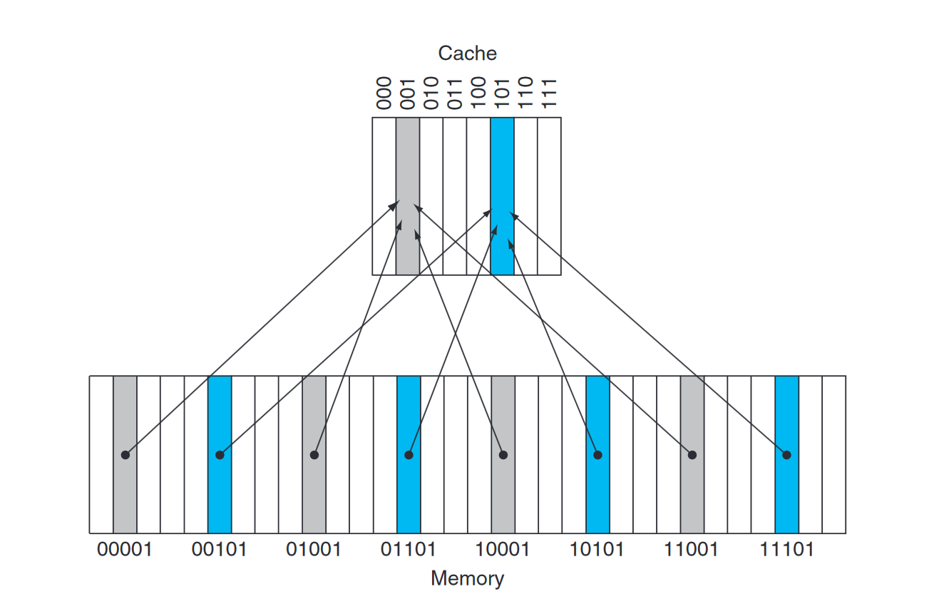
, which is multipile main memory blocks point to a same cache block.
Because each cache location may contains the contents of a number of different memory locations, how do we know whether a requested word is in the cache or not? We answer this question by adding a set of tags to the cache.
The tags contain the address information required to identify whether a word in the cache is the requested word. The tag needs just to contain the upper portion of the address, corresponding to the bits that are not used as an index into the cache. More specificly, those address mapped into the same address in the cache are differed in the upper portion of the address.
For example, in figure above showing collisions, we need only have the upper two of the five address bits in the tag, since the lower 3-bit index field of the address selects the block in cache. Architects omit the index bits because they are redundant, since by definition, the index field of any address of a cache block must be that block number.
We also need a way to recognize that a cache block does not have valid information. For instance, when a processor starts up, the cache does not have good data, and the tag fields will be meaningless. Even after executing many instructions, some of the cache entries may still be empty. Thus, we need to know that the tag should be ignored for such entries. The most common method is to add a valid bit to indicate whether an entry contains a valid cache address. If the bit is not set, there cannot be a match for this block.
The Big Picture
Caching is perhaps the most important example of the big idea of prediction. It relies on the principle of locality to try to find the desired data in the higher levels of the memory hierarchy, and provides mechanisms to ensure that when the prediction is wrong it finds and uses the proper data from the lower levels of the memory hierarchy. The hit rates of the cache prediction on modern computers are often above 95%